AD5679R


概览
High performance
High relative accuracy (INL): ±4 LSB maximum at 16 bits
TUE: ±0.14% of FSR maximum
Offset error: ±1.5 mV maximum
Gain error: ±0.06% of FSR maximum
Low drift 2.5 V voltage reference temperature coefficient:
2 ppm/°C typical40 mA short-circuit current
Wide operating ranges
−40°C to +125°C temperature range
2.7 V to 5.5 V power supply range
Simplified implementation
User selectable gain of 1 or 2 (GAIN pin)
1.8 V logic compatibility
50 MHz SPI with readback or daisy chain
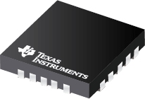
28-lead, 4 mm × 4 mm, RoHS compliant LFCSP
The AD5679R is a low power, 16-channel, 16-bit, buffered voltage output, digital-to-analog converter (DAC) that includes a 2.5 V, 2 ppm/°C internal reference (enabled by default), and a gain select pin, resulting in a full-scale output of 2.5 V (gain = 1) or 5 V (gain = 2). The device operates from a single, 2.7 V to 5.5 V supply range and is guaranteed monotonic by design. The AD5679R is available in a 28-lead lead frame chip scale package (LFCSP) and incorporates a power-on reset (POR) circuit that ensures that the DAC outputs power up to and remains at zeros-cale until a valid write. The AD5679R contains a power-down mode that reduces the current consumption to 2 μA typical when in power-down mode.
Applications
Optical transceivers
Base station power amplifiers
Process control (programmable logic controller (PLC) input/output cards)
Industrial automation
Data acquisition systems
Product Highlights
High channel density
16 channels in 4 mm × 4 mm LFCSPHigh relative accuracy (integral nonlinearity (INL))
±4 LSB maximumLow drift, 2.5 V, on-chip reference


